| |
|
|
|
|
|
Į║Ū╔─┌┼═(Spincoater)
ĖČĮ║┼®Š¾Č¾└╠│╩(Mask
Aligner) |
|
|
|
| |
|
| |
|
|
|
|
|
|
|
| TRANSFERS & SORTERS WAFER ALIGNERS VACUUM WANDS WAFER PICKS METAL CASSETTES MASK PICKS OPENERS PRESENTERS TRANSPORT BAGS MOCK WAFERS |
| |
|
|
|
|
|
|
|
| |
|
|
|
|
|
|
|
|
|
Automatic flat Aligner |
|
|
|
| |
Sorters
SafeGuard Thin/Compound
Automatic Slide Transfer
Manual Slide Transfer |
|
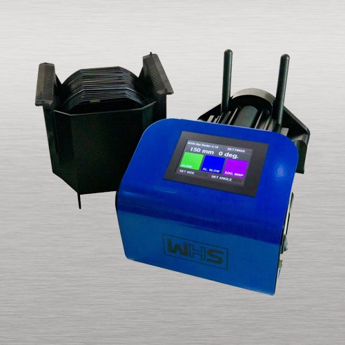
WHS-A1
Automatic Flatfinder
Wafer Size:3" 4" 6" 8"
Multi size :3"4"5"6" |
|
|
|
|
-Type:Automatic
-up to 25 slot
Material
Stage: Anti-Static polyoxymethylene
Roller: Anti-Static Polyurethane
|
| |
|
Automatic Notch Aligner
Automatic-flat-aligner
Manual-notch-aligner
Manual-flat-aligner |
Antistatic Construction With Wafer and Cassette Ground Paths
Quick Disconnect Roller for Easy Cleaning
+/- 1ĪŲ Primary Flat Alignment Accuracy
Applications: Alignment, Lot integrity and Edge inspection |
| |
|
Portable Wand
Vacuum Wand Set
Vacuum tips
Vacuum Handles |
|
 |
|
 |
.jpg) |
|
| |
|
|
Wafer 3-point mechanical gripper
Wafer Edge Pick |
Alignment - Wafer flat and notch aligners are used in the semiconductor industry to ensure that wafers are oriented correctly during various processes, such as lithography, deposition, and etching. The flat aligner has a notch or flat that corresponds to the orientation of the wafer's crystal lattice structure. This is critical because the orientation of the wafer affects the performance and functionality of the final semiconductor device |
| |
|
|
Aluminum Process Cassettes
Aluminum Box Cassettes
Stainless Steel Process Cassettes
Process Cassettes 300mm |
Lot integrity - Aligners are also used in the semiconductor industry to aid operators in performing lot integrity checks. By rotating the wafer scribe, which is the identification marking on the wafer's edge, to be visible to the operator, the operator can verify that the correct lot of wafers is being loaded into a production tool. This is an important step in preventing errors and ensuring consistent product quality. |
| |
|
|
Mask Pick - Side Grip
Mask Pick - Horizontal Grip |
Edge inspection - Wafer flat and notch aligners are also used in the semiconductor industry to inspect wafers for edge defects. This macro inspection procedure is usually done under a light source and involves examining the edges of the wafer for any chips, cracks, or other imperfections. This is an important step in preventing wafer breakage during subsequent processing steps, as edge defects can weaken the wafer and cause it to break or fail. By using wafer flat and notch aligners to identify and inspect these defects, operators can take steps to prevent further processing of defective wafers and avoid costly production delays |
| |
|
|
Manual Reticle SMIF Pod Opener, RSP150
Manual FOUP Opener, 300 mm |
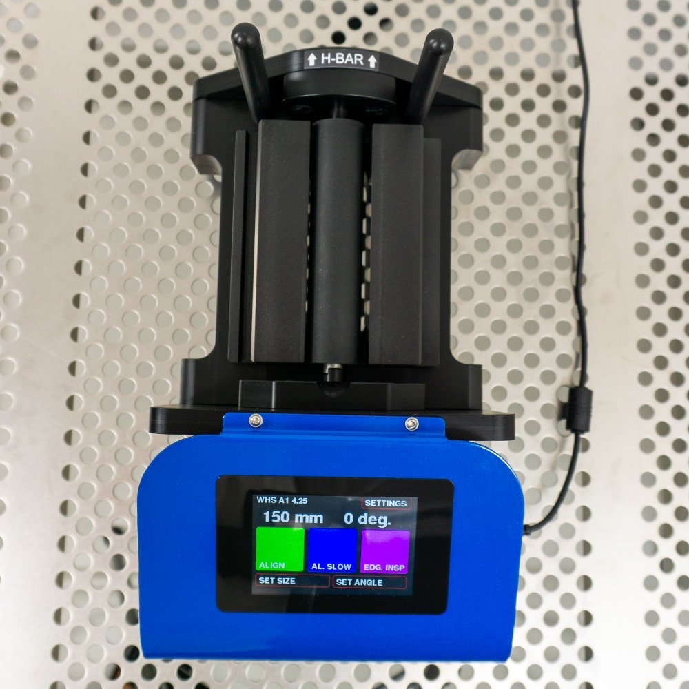
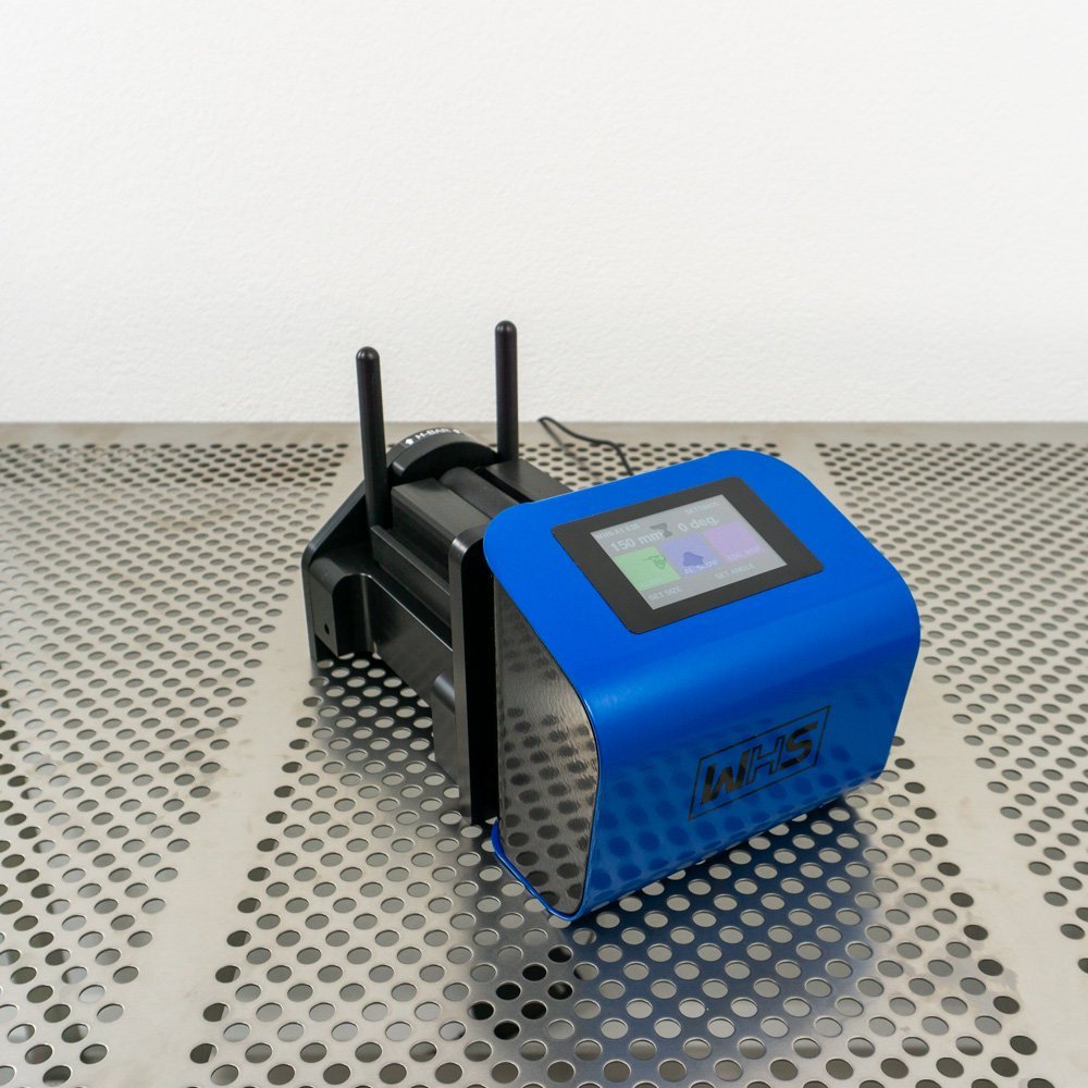
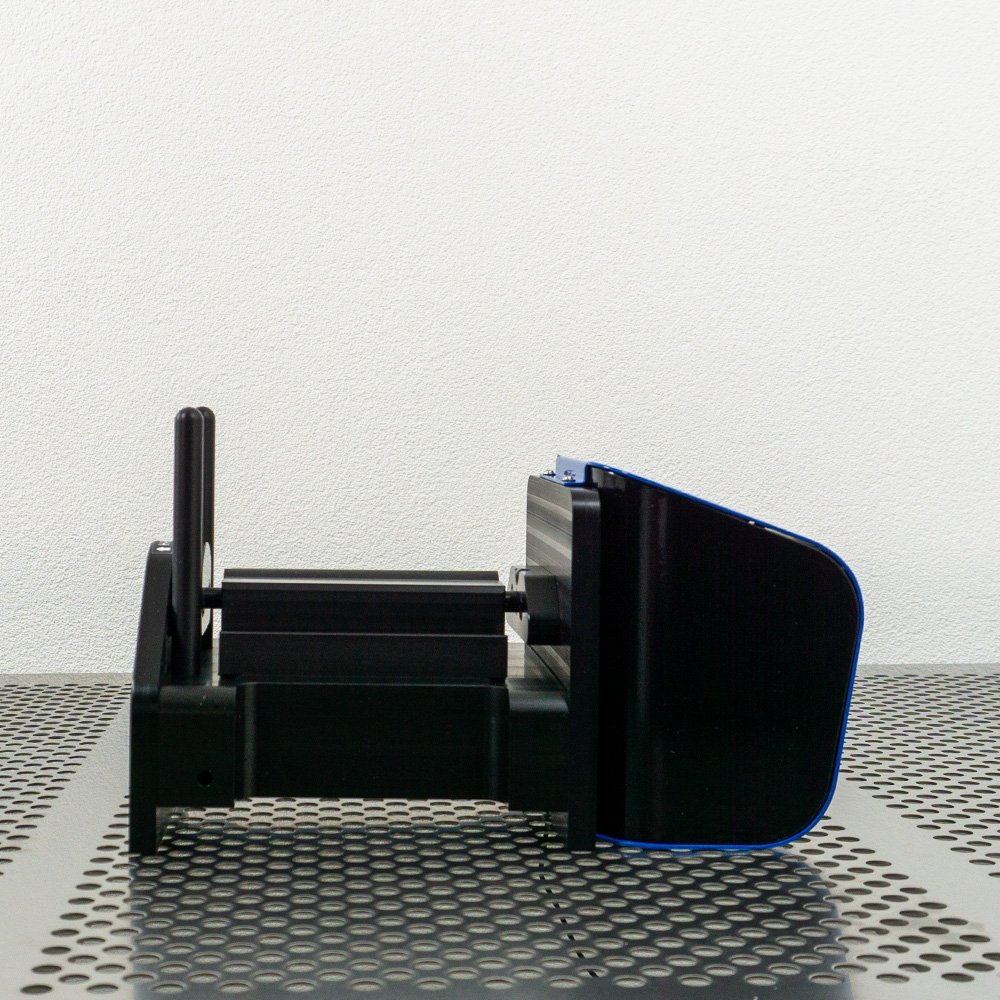
Advanced technology automatic wafer flat aligner for alignment 76 mm up to 150 mm wafers. Engineered for InP, GaAs, GaN and SiC compound wafer handling. Features motorized stage for gentle lifting of compound wafers - protecting the wafer edge and increasing yields; touchscreen recipe software for standard alignment, thin wafer/compound wafer alignment and edge inspection recipes. ISO Class 3. |
| |
|
|
Automatic Wafer Presenter
Manual Five-Wafer Lift Presenter
Manual Single Wafer Presenter
21-manual-wafer-escalators |
|
|
|
|
| |
└ń╝║ITS co.
░µ▒ŌĄĄ
Š╚ŠńĮ├ Ą┐Š╚▒Ė ╚Ż░Ķ 555-9 Š╚Šń
▒╣┴” └»┼ļ┤▄┴÷ 17Ą┐ 127╚Ż
Tel
: (031) 479-4211/2, Fax : (0504) 460-0288
1992-2023
,Jsi.co. All rights reserved
Contact us :contrabase26@gmail.com jsi@jsits.com |
| |
|
|
|
|
|
|
|



.jpg)